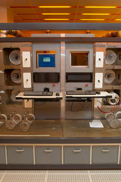
Equipment
The equipment set within the cleanroom includes tools to implement all of the processing steps typically used in the fabrication of electronic devices (such as transistors), optoelectronics (such as lasers and photodetectors), microfluidic devices, and novel nanodevices. These capabilities include high-resolution electron-beam lithography; several optical lithography techniques; deposition of metal, dielectric, and semiconductor films; etching of metals, dielectrics, and semiconducting materials by both wet and dry chemical processes; and metrology techniques to support these processes.
Lithography
Lithography tools provide a patterning technique where a light sensitive polymer (photoresist) is exposed to a spectrum of light (electron-beam or ultraviolet) that causes it to change its structure.
-
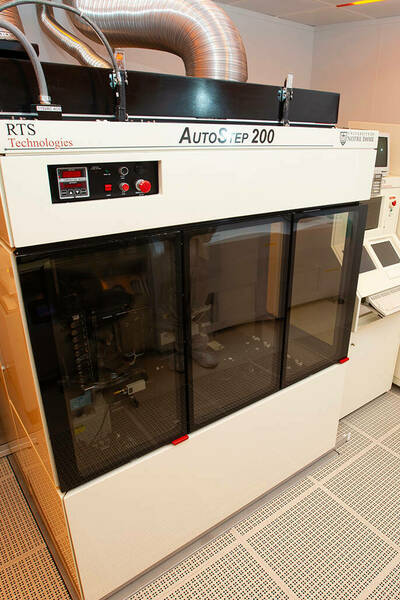
The AutoStep 200 lithography system is a 5x reduction, production grade i-stepper with repeat exposure capabilities as large as 17 mm x 17 mm.
-
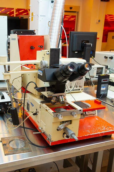
The SUSS MJB 3 mask aligner is equipped with a 200 W mercury short-arc lamp housing containing a relatively simple and yet comparatively high resolution optical system.
-
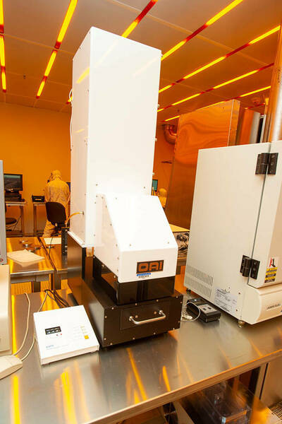
The OAI light source is a high-performance collimated illumination system intended for UV flood exposure related applications.
-
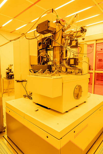
The Raith EBPG5200 is a state-of-the-art electron beam lithography system that can write to less than 8 nm in size on full 200 nm wafers or small sample pieces.
Deposition
Deposition systems grow films that are either conductive (metals) or non-conductive (dielectric) through a wide variety of physical and chemical vapor techniques.
-
The Denton Explorer® 14 e-beam evaporator is a six-pocket hearth deposition system.
-
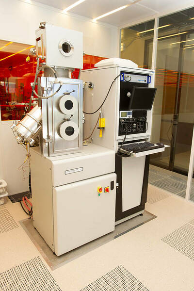
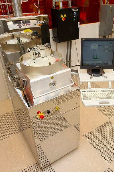
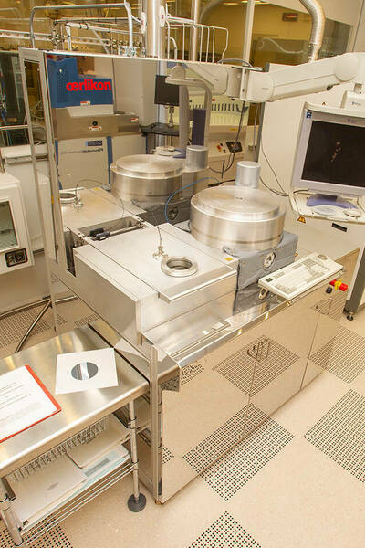
Dual-Chamber Sputtering System
The Oerlikon 450C Dual Chamber Sputtering System (DCSS) is a three-chamber, 16-target ultra-high vacuum (UHV) sputtering system used to deposit magnetic materials.
-
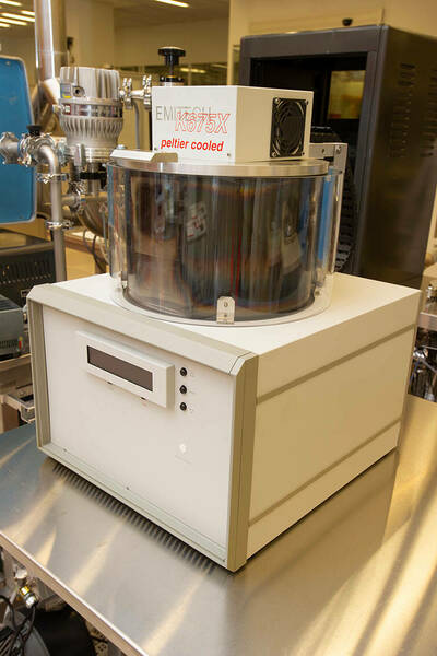
The K675X coating system employs a magnetron target assembly that enhances the efficiency of the sputtering process using low voltages, giving a thin and fine-grain coating.
-
The Model FC-1800 is an electron beam vacuum deposition system.
-
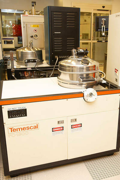
The Model FC-1800 is an electron beam vacuum deposition system.
-
The Model FC-1800 is an electron beam vacuum deposition system.
-
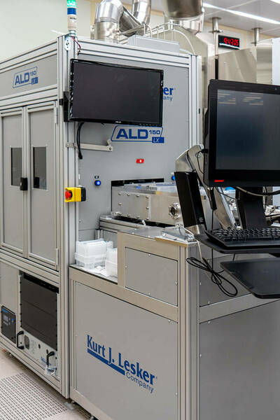
The Lesker ALD150LX Atomic Layer Deposition (ALD) system is designed for R&D applications using their patented precursor focusing technology and advanced process capabilities.
-
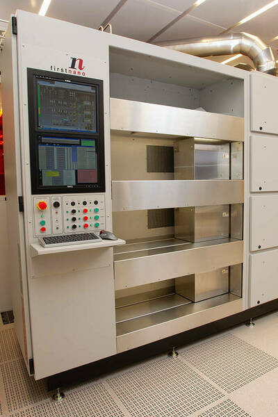
The First Nano EasyTube 6000 is a horizontal-tube furnace system, capable of processing 4" (100 mm) diameter silicon wafers.
-
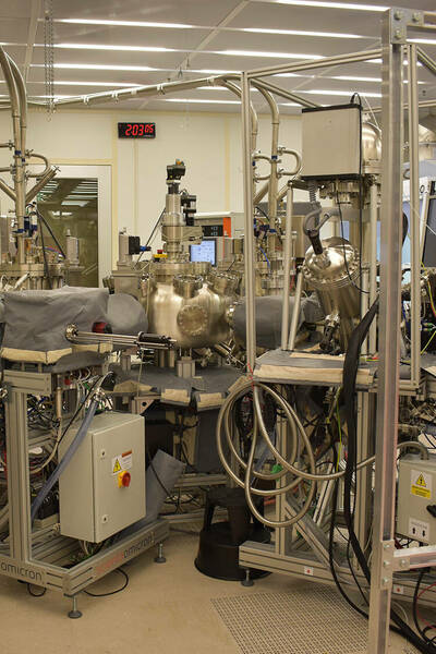
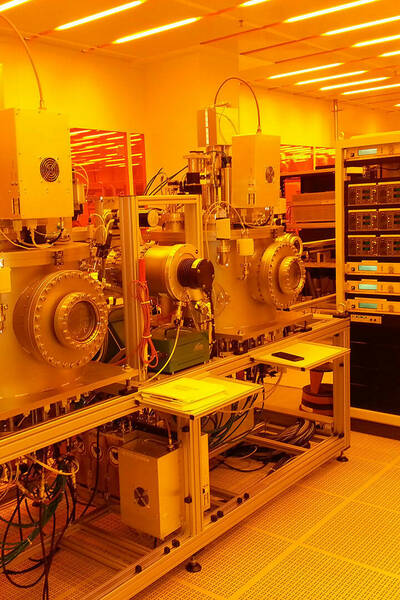
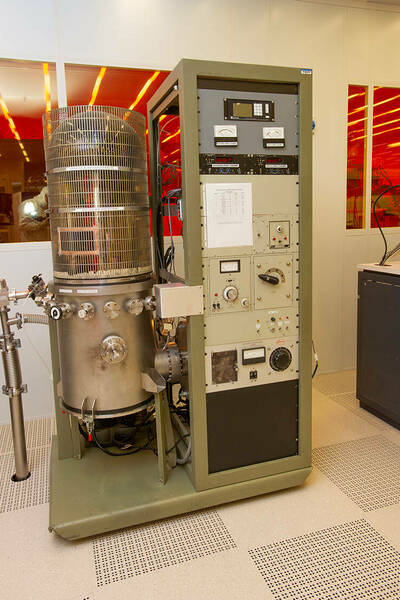
Molecular beam epitaxy (MBE) systems are used to grow high-purity, single-crystal films in specific crystallographic orientations determined by the substrate.
-
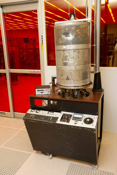
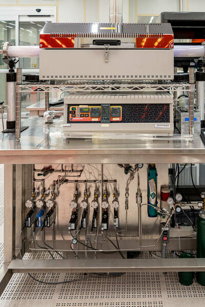
The metal organic chemical vapor deposition (MOCVD) system is used to create high purity crystalline compound semiconductor thin films like GaN.
-
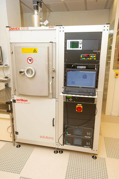
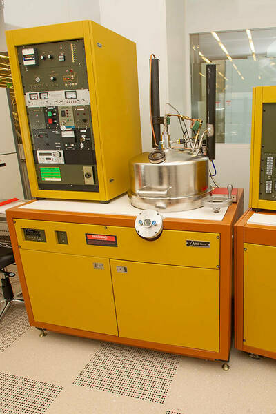
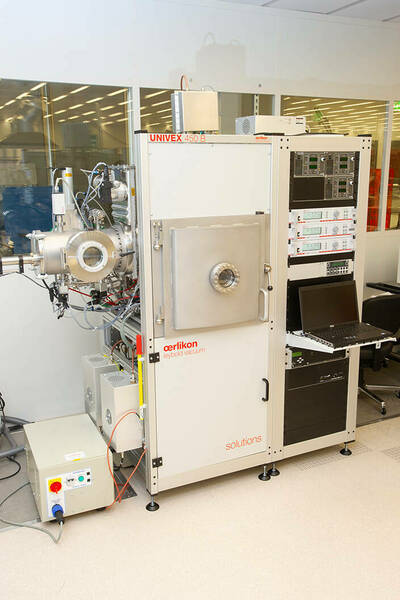
The Oerlikon 450B evaporator is an electron beam vacuum deposition system.
-
The Oxford Instruments FlexAL atomic layer deposition system is a plasma-enhanced ALD system for the monolayer growth of thin films.
-
The Randex Model 2400-8SA sputtering system is designed to deposit a wide variety of materials onto substrates
-
The Unaxis 790 Series Plasma Enhanced Chemical Vapor Deposition (PECVD) system is used for the deposition of SiO2 and silicon nitride on a wide variety of substrates and wafers.
-
The Savannah 100 is an atomic layer deposition (ALD) tool.
-
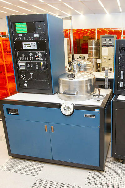
Single-Chamber Sputtering System
The Oerlikon 450B Single Chamber Sputtering System (SCSS) is equipped with three DC magnetron-enhanced sputtering guns (800 W) and two RF sputtering guns (300 W).
-
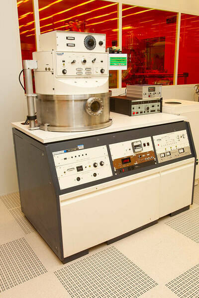
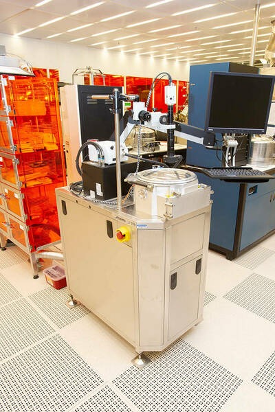
Varian Thermal Deposition System
The Varian thermal evaporator is a thermal vacuum deposition system.
-
The unit is used for thermal vacuum deposition of Al or Cr to the substrates situated some 30 cm above the evaporating metals.
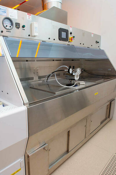
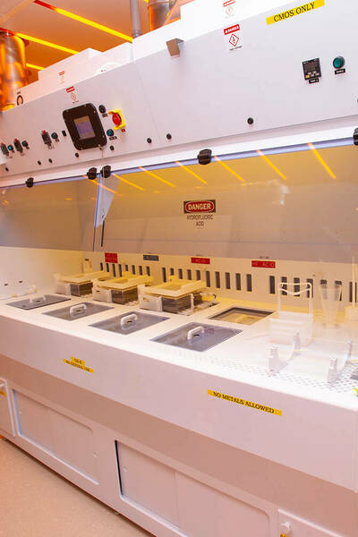
Etching
Dry (plasma) etching is the process of removing unwanted material from a substrate by converting the unwanted material into a volatile gas phase.
-
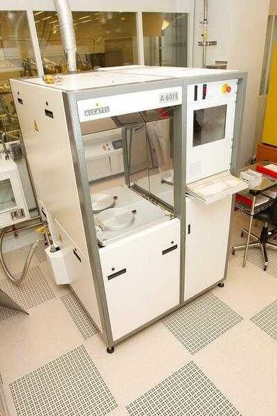
The Alcatel 601 E is an automatic etching machine used exclusively for the plasma etching of silicon and related materials utilizing the Bosch Process.
-
The Drytek Mega Strip 5 utilizes an exclusive passivation method, which produces a greater number of active species.
-
The MemsStar is a vapor-phase silicon etch system using xenon difluoride (XeF2) and a novel vapor delivery system.
-
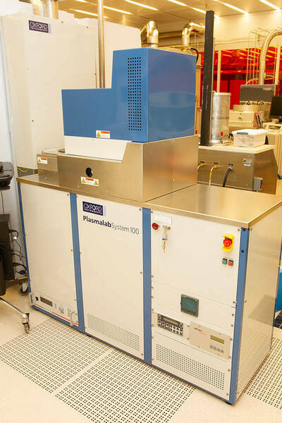
The Oerlikon system is an inductively coupled plasma (ICP) reactor that is used for reactive ion etching.
-
The Oxford system is an inductive coupled plasma (ICP) reactor that is used for reactive ion etches.
-
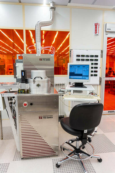
Plasma-Therm's 790 Series provides a platform for parallel plate (capacitively coupled) reactive ion etch (RIE) processes.
-
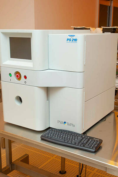
The PS210 utilizes high-energy microwaves as its energy source for ion/radical formation.
-
The Tegal PlasmaLine asher is a general purpose O2 plasma used to remove photoresist and for general purpose cleaning.
-
Model 144AX produces near-atomically clean surfaces in less than one minute by utilizing the UV/ozone cleaning method.
Thermal Processes
Thermal processing equipment relies on heat to achieve diffusion, activation (dopants), or annealing of substrates.
-
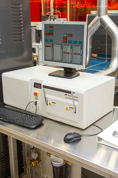
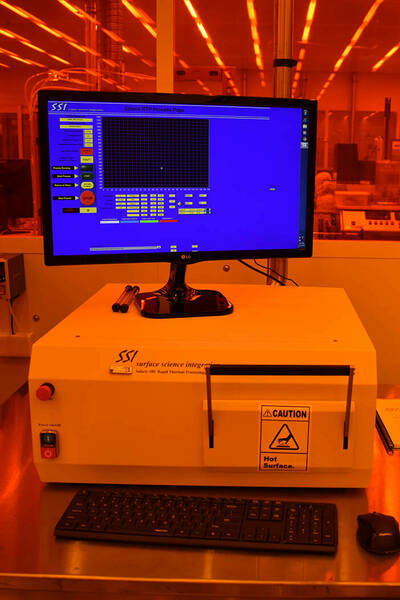
The AccuThermo AW610 is an atmospheric rapid thermal processing (RTP) system that uses high-intensity visible radiation to heat single wafers for short process periods of time at precisely controlled temperatures.
-
This furnace is typically used for metal annealing to produce ohmic contacts and curing (spin on glass and BCB resists).
-
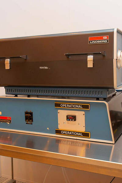
The Carbolite nanotube furnace is a three-zone heating system with a max temperature of 1200 °C.
-
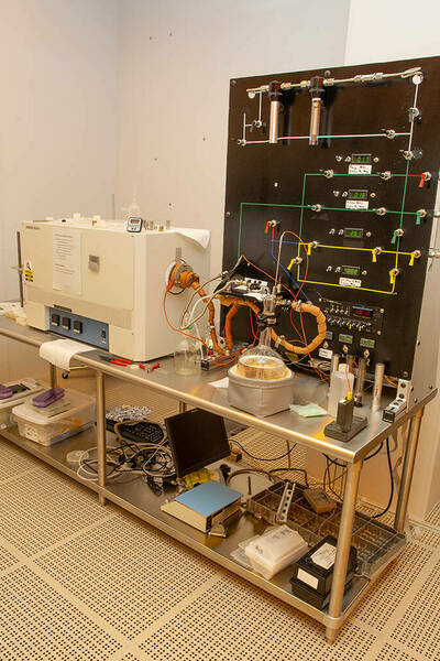
The III-V oxidation furnace is used for the formation of compound semiconductor oxide films.
-
The Solaris 75/100 is an RTP system designed for R&D and pre-production.
-
The six-stack Thermco Furnace is used for general purpose silicon processing.
Planarization and Mechanical Processing
This equipment provides material removal and polishing applications used to thin substrates, control surface roughness, or smooth substrate surfaces using colloidal suspensions and abrasive pads.
-
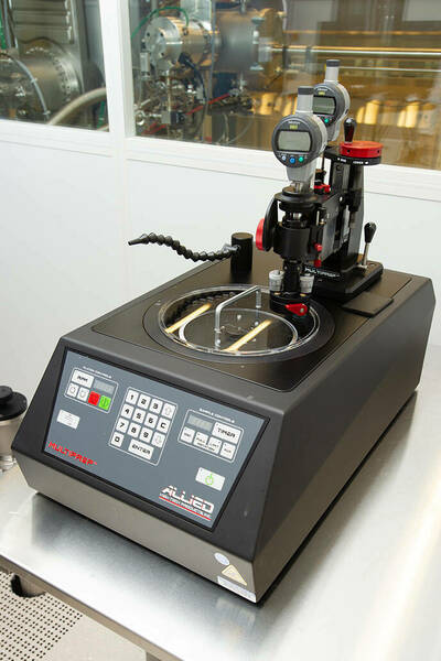
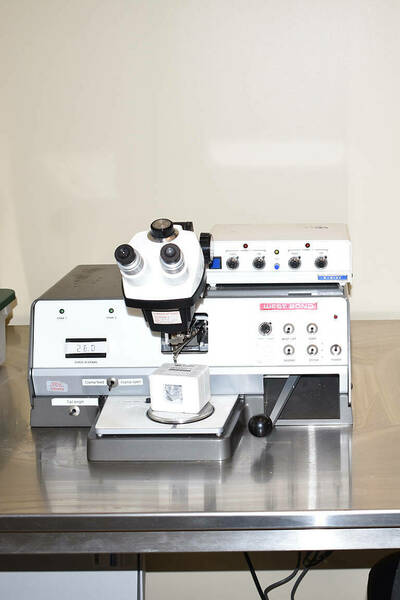
The MultiPrepTM System enables precise semi-automatic preparation of a wide range of materials for microscopic evaluation and package thinning applications.
-
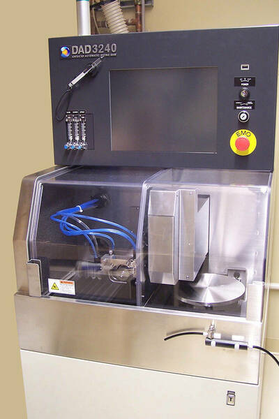
The Disco Automatic Dicing Saw (Model DAD 3240) is a programmable automatic saw for cutting semiconductor wafers and other hard materials.
-
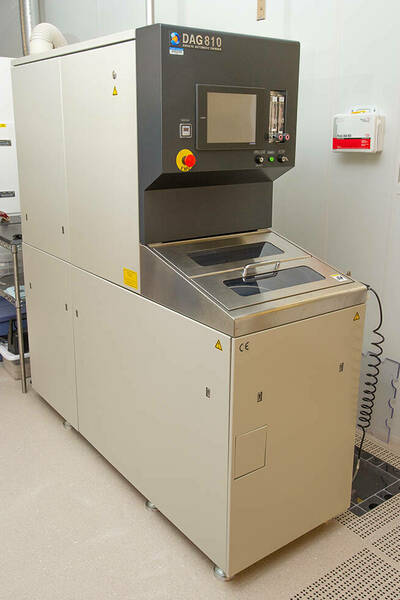
The Disco Automatic Grinder Model 810 (DAG 810) is a single-spindle / single-chuck-table unit that performs back-side grinding on samples.
-
Hall Effect Measurement System
The HL5500PC enables measurement of resistivity, carrier concentration and mobility on a wide range of semiconductors and with minimum effort in sample preparation.
-
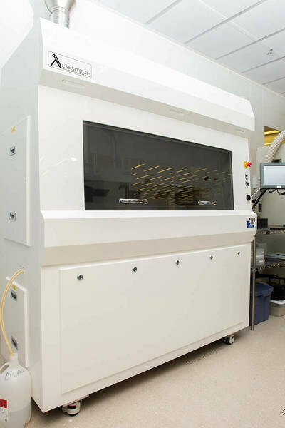
The Logitech Orbis Chemical Mechanical Planarization (CMP) system is used for fine-scale polishing and planarization of a variety of metals in the damascene process as well as dielectrics.
-
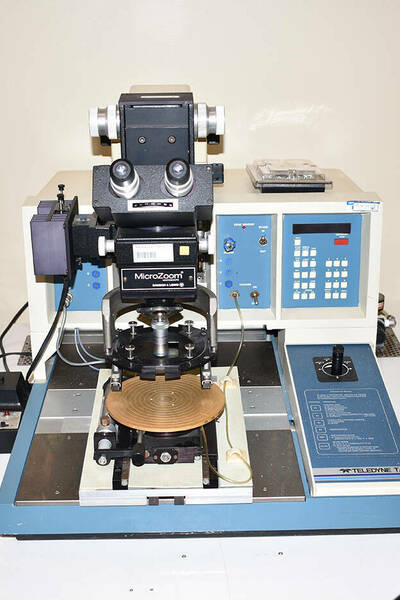
The Teledyne TAC probe station allows testing of devices that are still mounted on a wafer.
-
NDNF users have access to the model 7372E die bonder, the model 7400E wedge bonder, and the model 7400A wire bonder.
Characterization
Once devices and films are created, characterization instruments are used to measure or acquire data on their properties.
-
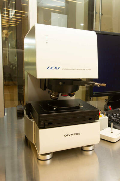
The Olympus LEXT OLS4000 is a confocal laser (405 nm) microscope capable of taking high-resolution 3D images.
-
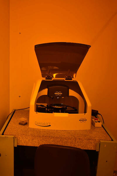
The DektakXT® stylus profilometer features a revolutionary benchtop design that enables critical nanometer-level surface measurements with an unmatched repeatability of 4 Å and up to 40% improvement in scanning speeds.
-
Filmetrics Thin Film Measurement System
The Filmetrics F40 is uses spectral reflectance to measure the thickness of transparent and semi-transparent thin films.
-
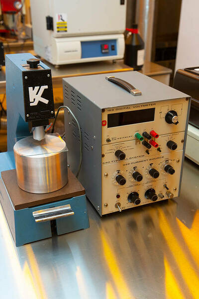
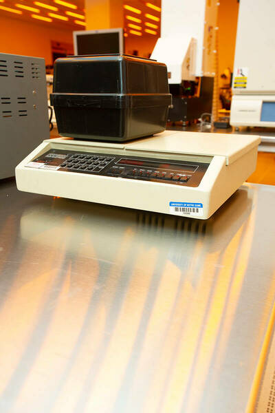
The Kulicke and Soffa Model 3007 four-point in-line probe is used in conjunction with a Keithley model 530 Type-All system to make applicable characterization measurements.
-
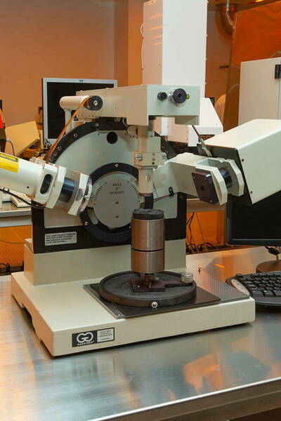
The L117 Ellipsometer has provisions for precise, pin-located setting of the angle of incidence between 45 and 90 degrees.
-
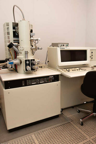
This Hitachi S-4500 field emission scanning electron microscope (FESEM) is capable of producing high-resolution images between 20k and 500k.
-
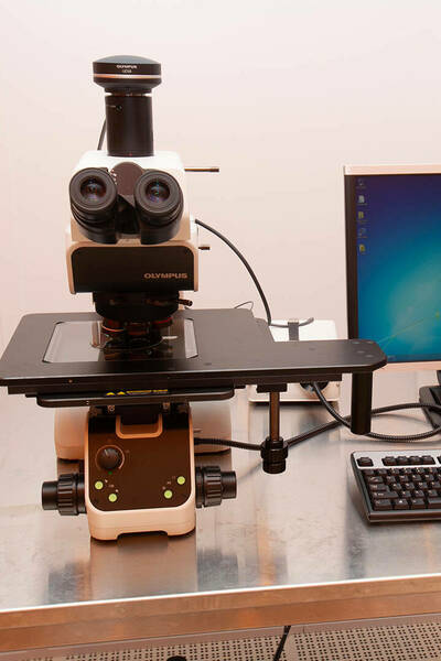
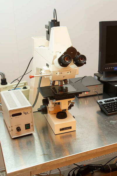
Various optical microscopes are available for use in the lab with magnifications ranging from 2.5x up to 100x.
-
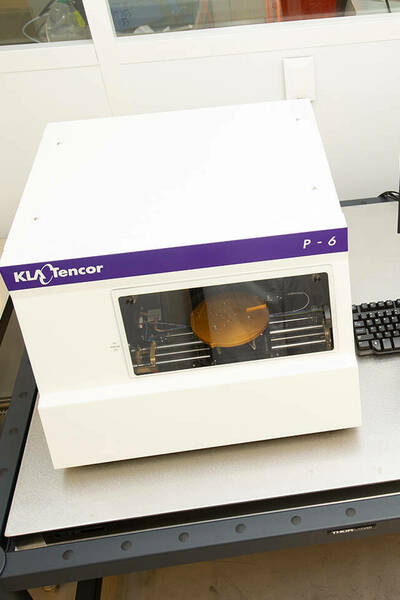
The P-6 offers complete high-resolution 2D and 3D analysis of surface topography in a versatile platform.
-
Semiconductor Parameter Analyzer
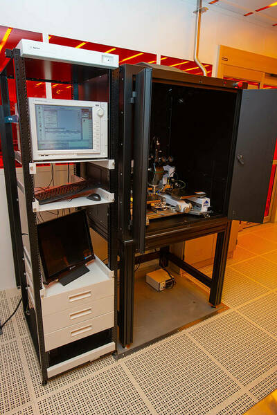
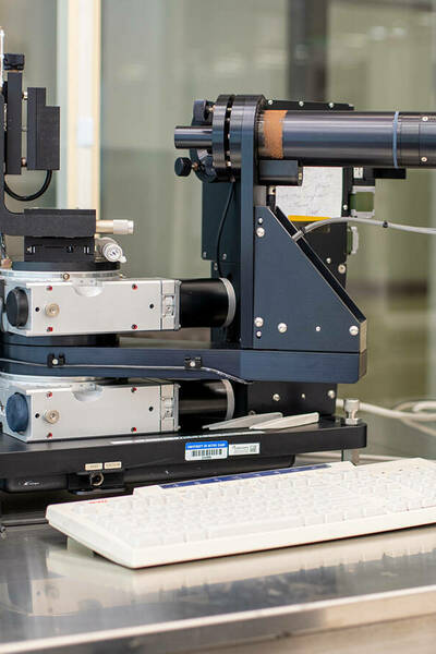
The M150 Measurement Platform is a high-performance probing station that allows for precision electrical measurements, from DC to high-frequency RF.
-
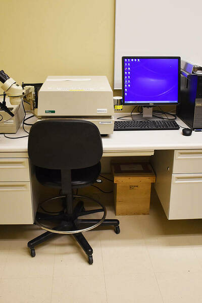
The Variable Angle Spectroscopic Ellipsometer (VASE®) is a totally automated, thin film characterization system that uses high-precision angle, and a wide spectral range (240 to 1700 nm).
-
The FPP 5000 is a four-point probe used for the measurement of resistive properties of semiconductor wafer and resistive films.
Additional Capabilities
These additional tools can be used for device fabrication.
-
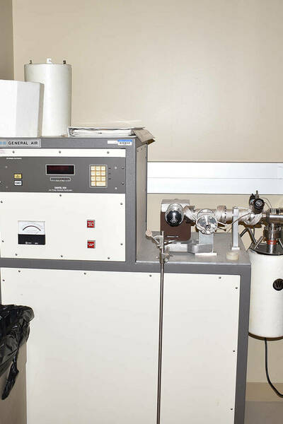
The ampoule sealing station is a vacuum sealing system that encapsulates samples in a small quartz vial and applied high temperatures to melt the quartz vials and form an airtight seal.
-
The E3100 is used for the critical point drying biological and geological specimens and the controlled drying of MEMs, aerogels and hydrogels.
-
The MOS clean bench and its Teflon contents are used exclusively for cleaning of metal oxide semiconductor structures.
-
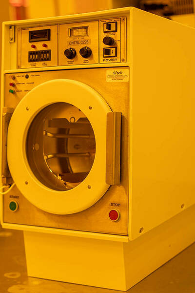
The Sitek spin rinse dryer is a compact tabletop dryer that is capable of processing 4" wafers.