Facilities
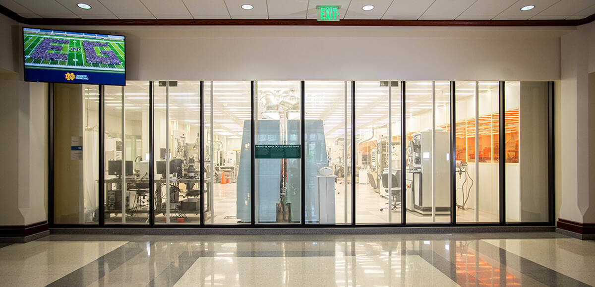
The Notre Dame Nanofabrication Facility (NDNF) is the equipment set and supporting cleanroom environment for research and teaching in nanoelectronics, optoelectronics, microfluidics, nanofabrication, and related disciplines. The facility consists of a 9,000 square foot cleanroom and a full complement of processing and test equipment necessary for fabricating and analyzing the performance of advanced devices.
The NDNF is divided into three main areas:
- The ISO 7 (class 10,000) zone is approximately 1,200 square feet, and houses back-end-of-line processes such as chemical-mechanical polishing (CMP), wafer thinning, packaging, as well as molecular beam epitaxy (MBE).
- The ISO 6 (class 1000) zone is approximately 2,500 square feet and contains the majority of the chemical vapor deposition (CVD) and physical vapor deposition (PVD) equipment, plasma etching systems, and a selection of characterization tools.
- The ISO 5 (class 100) zone measures 2,700 square feet and houses a range of lithography systems, including an electron beam lithography (EBL) tool, I-line projection lithography, contact printing, and direct-write optical lithography systems. Oxidation furnaces and metrology tools are also located in this zone.
The zones are classified by their "cleanliness" as measured by the number of particles per cubic foot of a specific particle size. This means that air in the class 100 area has fewer than 100 particles larger than 0.5 µm in diameter per cubic foot of air. (As a reference, typical outside air in an urban environment contains over 1 million particles per cubic foot, and is thus 10,000 times less clean than air within the NDNF.)
Learn More About the NDNF Design View the Facility Layout
Equipment Portfolio
The NDNF is a CMOS and III-V semiconductor fabrication facility as well as a MEMS and microfluidics facility. Lithography capabilities include contact and I-line projection optical lithography, direct-write maskless optical lithography, and a 100 kV electron beam direct-write EBL.
The etching capabilities include reactive-ion etching (RIE), multiple inductively-coupled RIE systems, a DRIE system for MEMS fabrication, and several plasma cleaning systems.
Deposition capabilities consist of multiple electron-beam evaporators, thermal evaporators, and several systems for both DC and RF magnetron sputtering of a wide range of metal and dielectric materials. Chemical vapor deposition (CVD) systems include plasma-enhanced chemical vapor deposition (PECVD), atomic layer deposition (ALD), plasma-enhanced ALD, and low-pressure (LPCVD).
Characterization capabilities include ellipsometry, step profilers, a thin-film measurement system, and an analytical probe station for electrical characterization of devices. In addition, a full suite of Olympus microscopes, from stereo zoom to a confocal system, and Hitachi S4500 scanning electron microscope providing 5 nm resolution, are available. Each microscope is connected to a high-resolution camera along with a line width measurement system.
Back-end-of-line processing includes chemical-mechanical polishing (CMP), lapping and polishing, backside grinding/thinning, dicing/singulation, and several wire bonding and die attach systems.